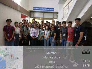
Department of Electronics and Telecommunication Engineering is collaboration with IETE SAKEC organized a visit to Nanofabrication facility, IITB on Saturday, 28/10/2023 for TE EXTC students. This visit was carried out for students to make them aware of different Fabrication processes involved in VLSI Design and the facilities available at IITB.
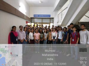
31 students with two faculty members Mr. Shridhar Sahu and Mrs. Gauri Chavan visited the facility which consisted of clean rooms, lithography equipment, sputtering process, molecular beam epitaxy and many more.
At IITBNF, there is a class 1000 cleanroom that has a maximum of 1000 foreign particles per cubic feet of air inside. The lithography process is used to write patterns on a resist layer (Photo lithography and Electron beam lithography) and the technique needed to transfer these patterns from the resist onto the main layer of the semiconductor wafer (Wet etching and Dry etching). Students also learnt about oxidation, thin film deposition and sputtering. All in all, it was a wonderful learning experience. The visit took 3 hours to be completed. The overall feedback from students was very motivating.
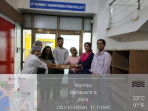
Before leaving the campus, a token of appreciation was presented to the IITBNF team for guiding the group of students and faculties throughout the visit.