 PCB Designing: Zero to Hero
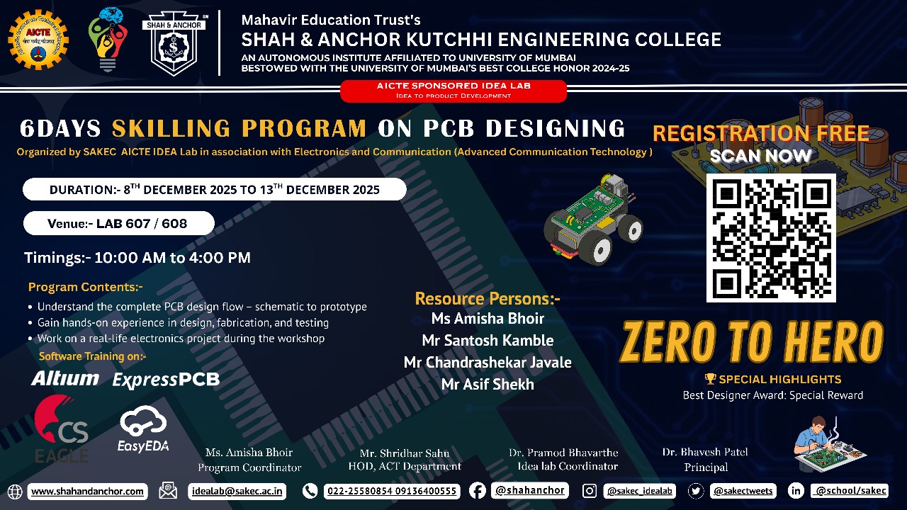
We’re excited to announce the upcoming 6-Day Hands-On Skilling Program on PCB Designing, organized by SAKEC AICTE IDEA Lab in collaboration with Electronics and Communication
(Advanced Communication Technology) Department.
This intensive skill-building program is designed to take students from basic circuit design concepts to professional-level PCB fabrication, helping them gain both software expertise and real-world hardware experience through guided training sessions and live demonstrations.
 Dates: 8th – 13th December 2025
 Time: 10:00am – 4:00 pm
 Venue: Lab 607/608
 Workshop Highlights:
 Day 1–2: Software Training on LTM, Eagle software, PCB Express, easyEDA tool. Day 3–4: Manual PCB Making – from circuit layout to etching and drilling. Day 5: Project Development Day – apply all your learning to design and build your own working project. Day 6: Project Exhibition & Evaluation
 Get trained directly by industry experts on latest PCB design tools and fabrication techniques
Speakers:-
Ms Amisha Bhoir
Mr Santosh Kamble
Mr Chandrashekar Javale
Mr Asif Shekh
 Learning Outcomes:
Participants will:
 Understand the complete PCB design flow – schematic to prototype Gain hands-on experience in design, fabrication, and testing Work on a real-life electronics project during the workshop Receive a certificate of completion under the SAKEC AICTE IDEA Lab
 Why You Should Join:Learn industry-standard EDA tools and PCB workflowsEnhance your hardware and embedded design skillsBoost your technical profile and project-building confidenceCompete for “Best PCB Designer” recognition
  Special Highlights
 Best PCB Design
 Limited Seats Available — Register Early!
Registration Link :- https://forms.gle/
For More details, Contact:
Ms. Amisha Bhoir – 9326000953 (Faculty Co-Ordinator )
Mr. Manav Kothari – 9820966945 (Student Co-Ordinator )