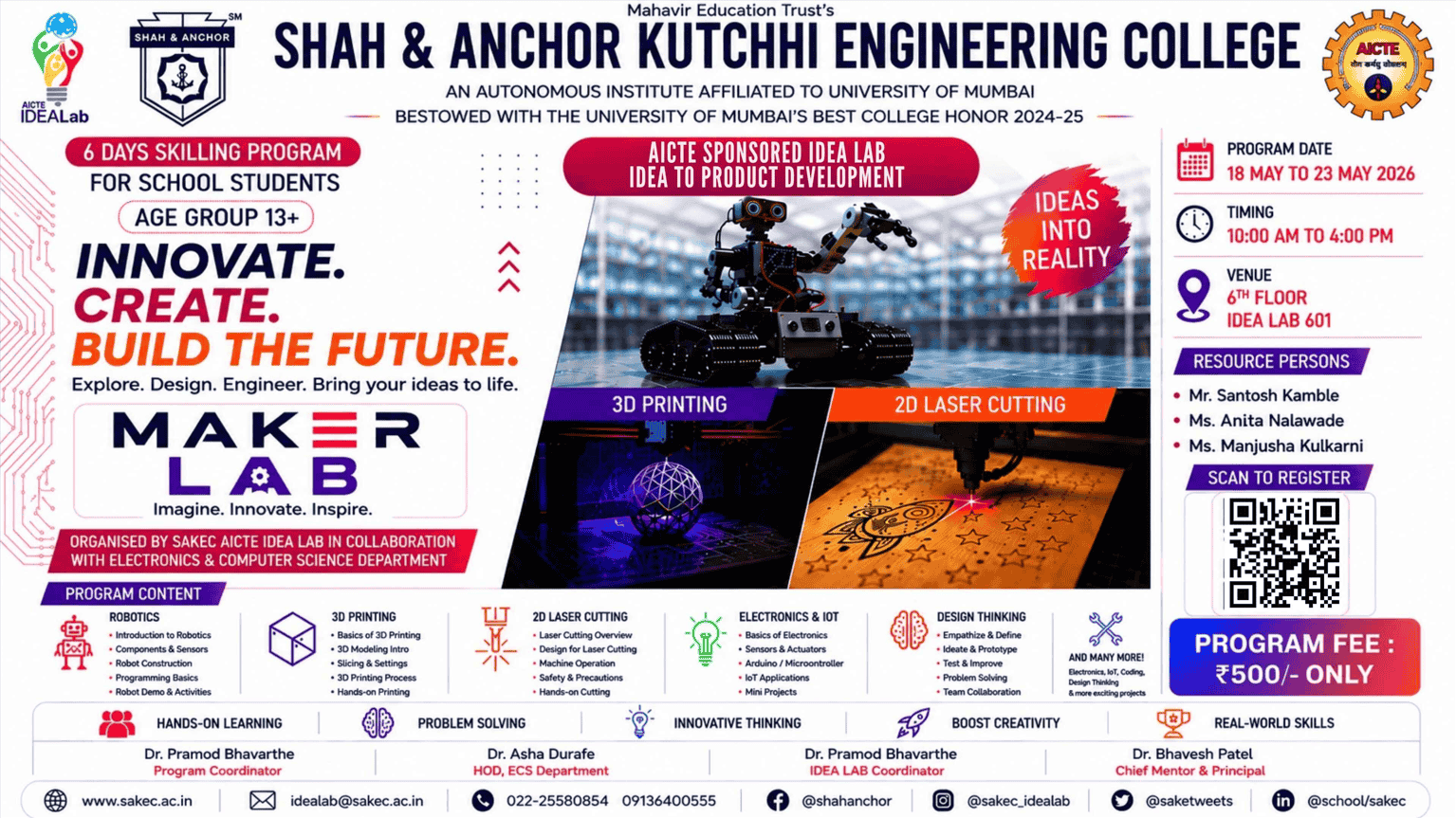
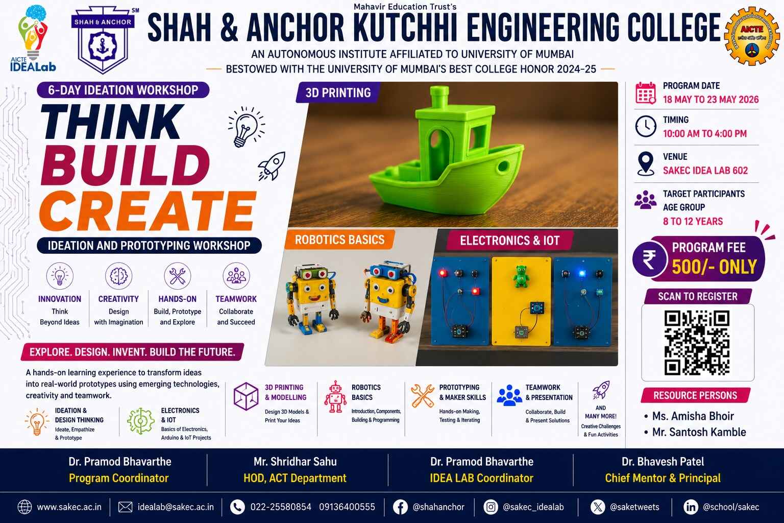
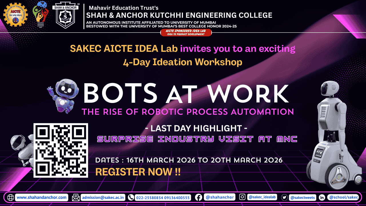
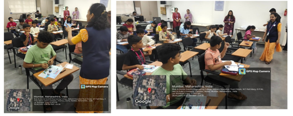
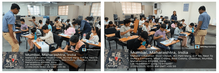
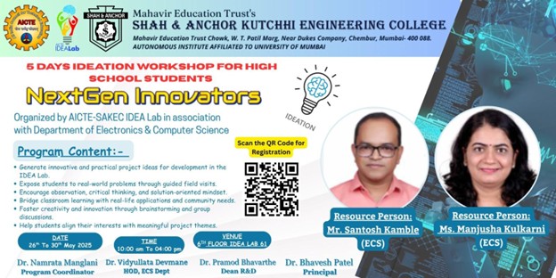
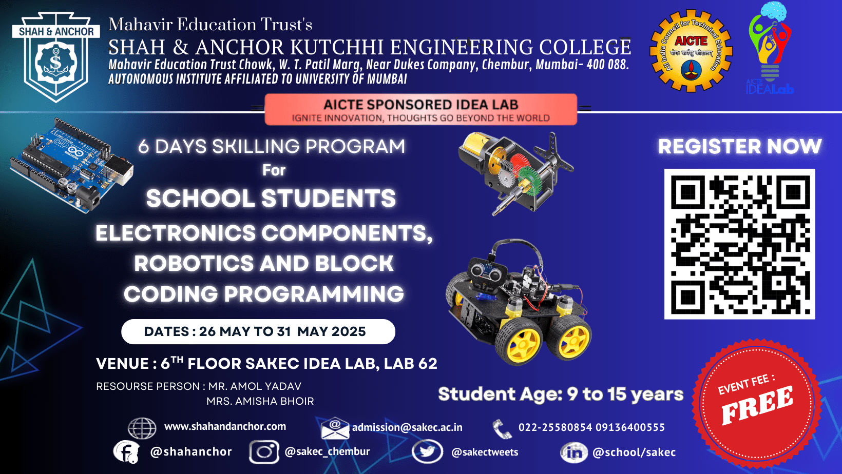
6 Days Skilling Program for School Students (Age Group 13+)
Event Name:
18 May 2026 to 23 May 2026
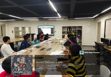
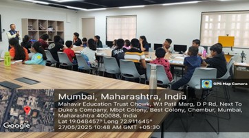
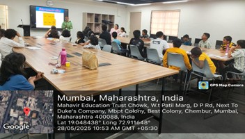
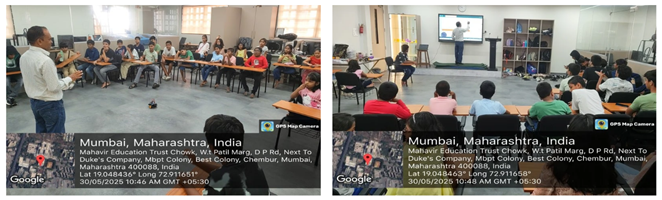
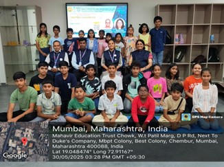
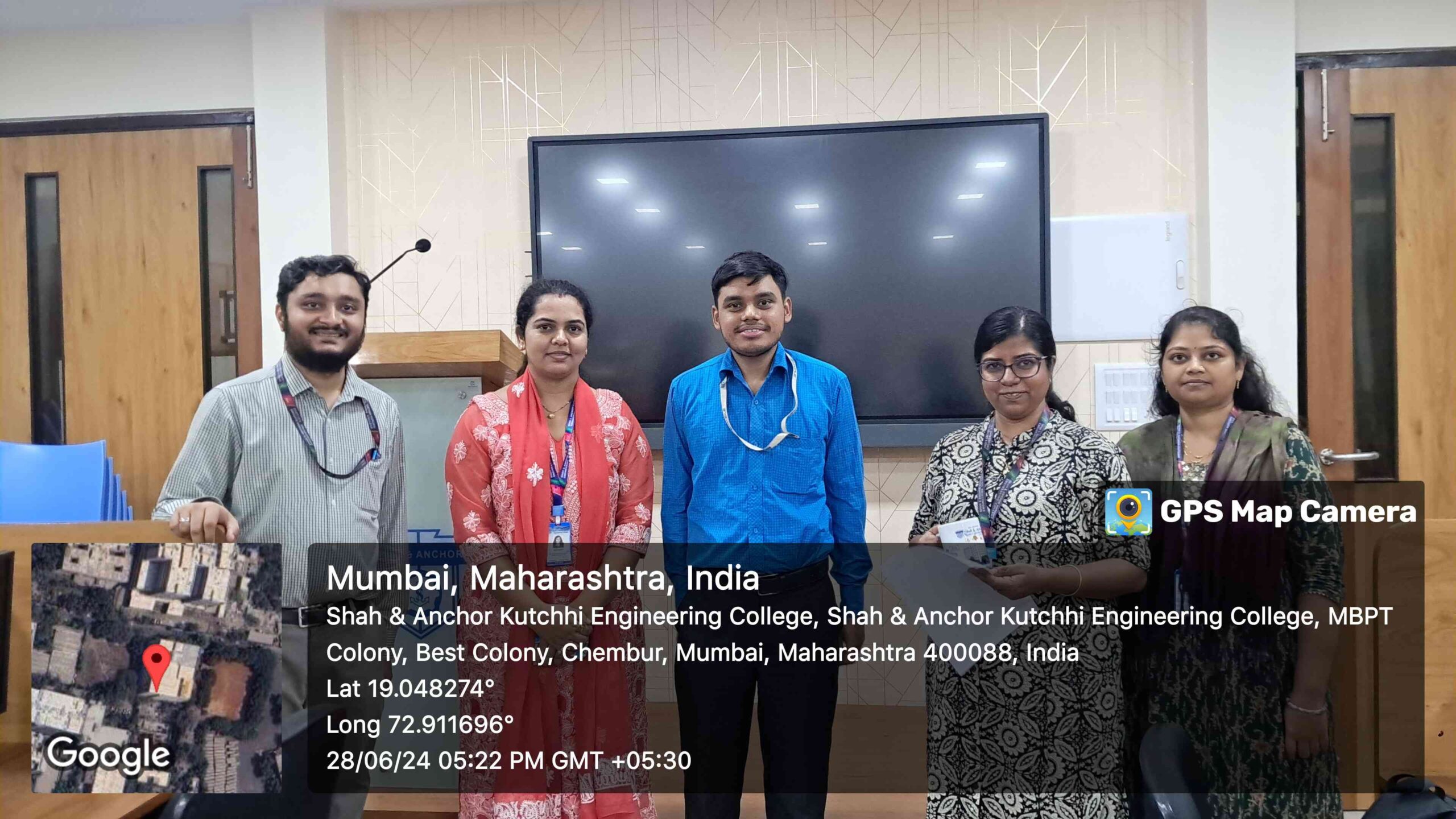
we are pleased to inform you that SAKEC AICTE IDEA LAB in collaboration with the Department of Electronics & Computer Science, Shah & Anchor Kutchhi Engineering College, is organizing a 6 Days Skilling Program for School Students (Age Group 13+) during 18 May 2026 to 23 May 2026 in offline mode.
Program Activities:-
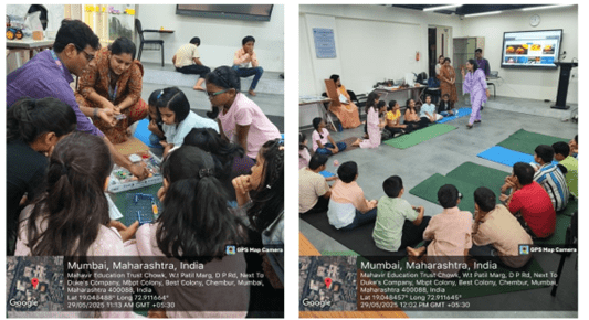
01. Basic Robotics Activities
02. Fun Electronics Experiments
03. Introduction to 3D Printing
04. Laser Cutting Demonstration
05. Simple Coding Activities
06. Creative Design Sessions
07. Mini Hands-on Projects
08. Team Activities & Innovation Games
What Students Will Learn:-
01. Basics of Robotics
02. Introduction to Sensors & Electronics
03. Creative Thinking & Problem Solving
04. Basics of 3D Printing
05. Simple Design & Making Activities
06. Teamwork & Communication Skills
07. Innovation through Hands-on Learning
Duration:
6 Days Program – 18/05/2026 to 23/05/2026
Mode of Conduction:
OFFLINE in AICTE SAKEC IDEA LAB
LOCATION:-
SAKEC AICTE IDEA LAB – IDEA LAB 601, 6th Floor
Shah & Anchor Kutchhi Engineering College, Chembur.
Timings:
10:00 AM to 4:00 PM
Program Fee:
Rs. 500/- Only per participant.
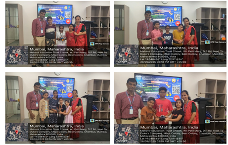
Take-Away :-
- Hands-on Learning Experience
- Creativity & Innovation Exposure
- Fun Learning Activities
- Certificate upon Successful Completion
- Mini Project Demonstration
HURRY SINCE SEATS ARE LIMITED, ENROLLMENT ON FIRST COME FIRST SERVE BASIS.
For more details contact:
Mr. Santosh Kamble- 9029975757
Mr. Ganesh Nikam – 8169737834
Email: idealab@sakec.ac.in
Registration Google Form Link:
[https://forms.gle/
 Warm Regards,
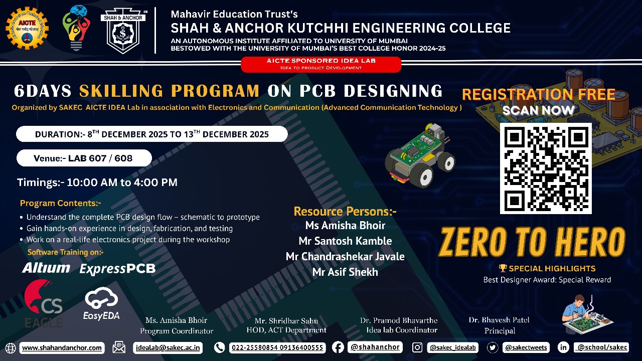 PCB Designing: Zero to Hero
 Dates: 8th – 13th December 2025
 Time: 10:00am – 4:00 pm
 Venue: Lab 607/608
 Workshop Highlights:
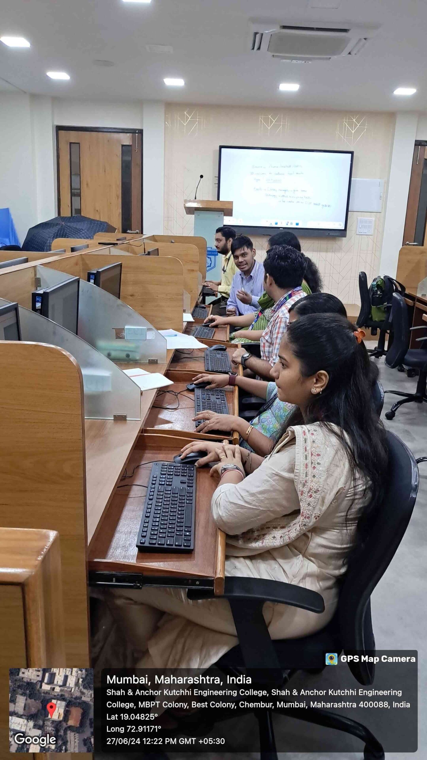
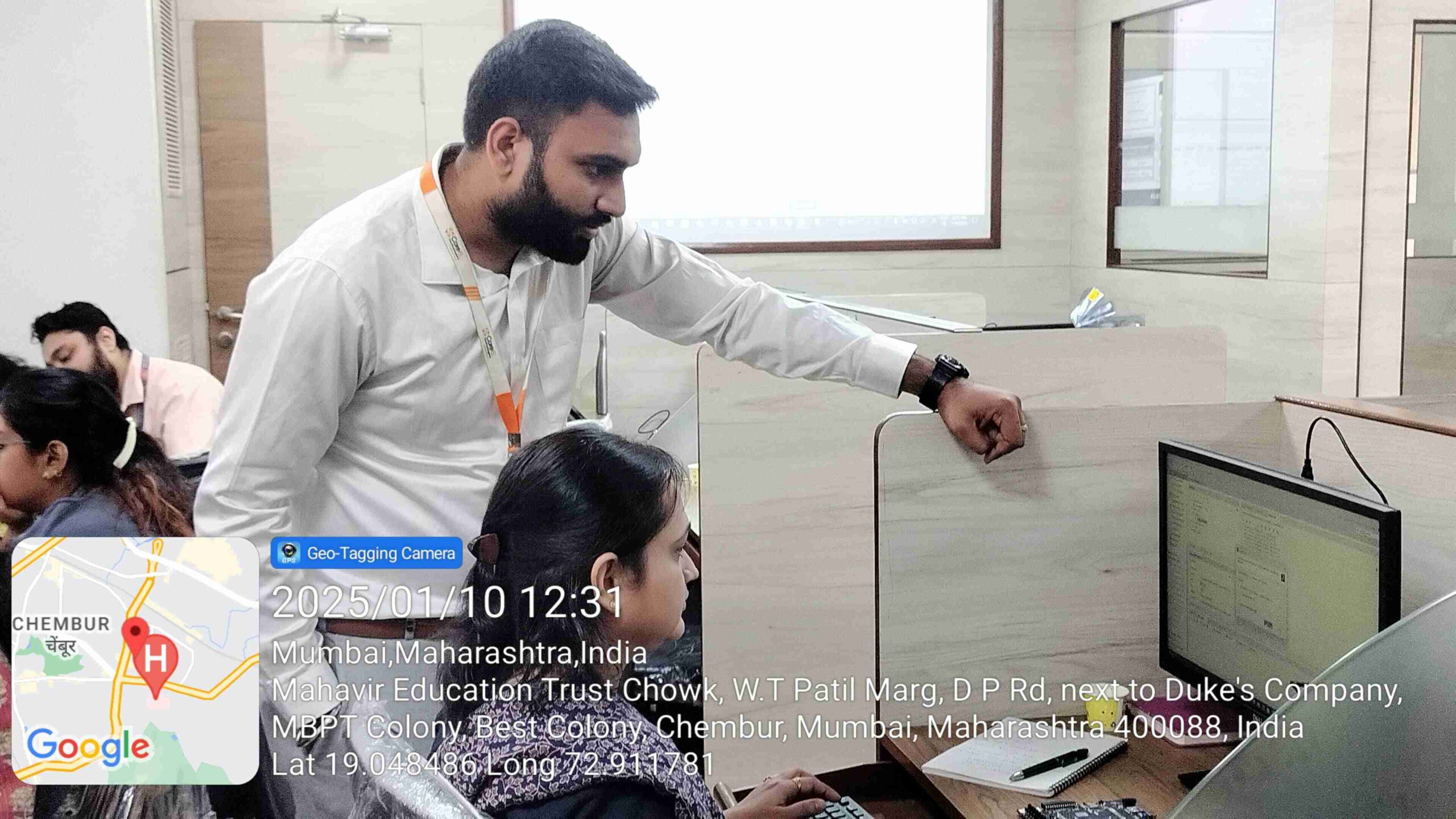
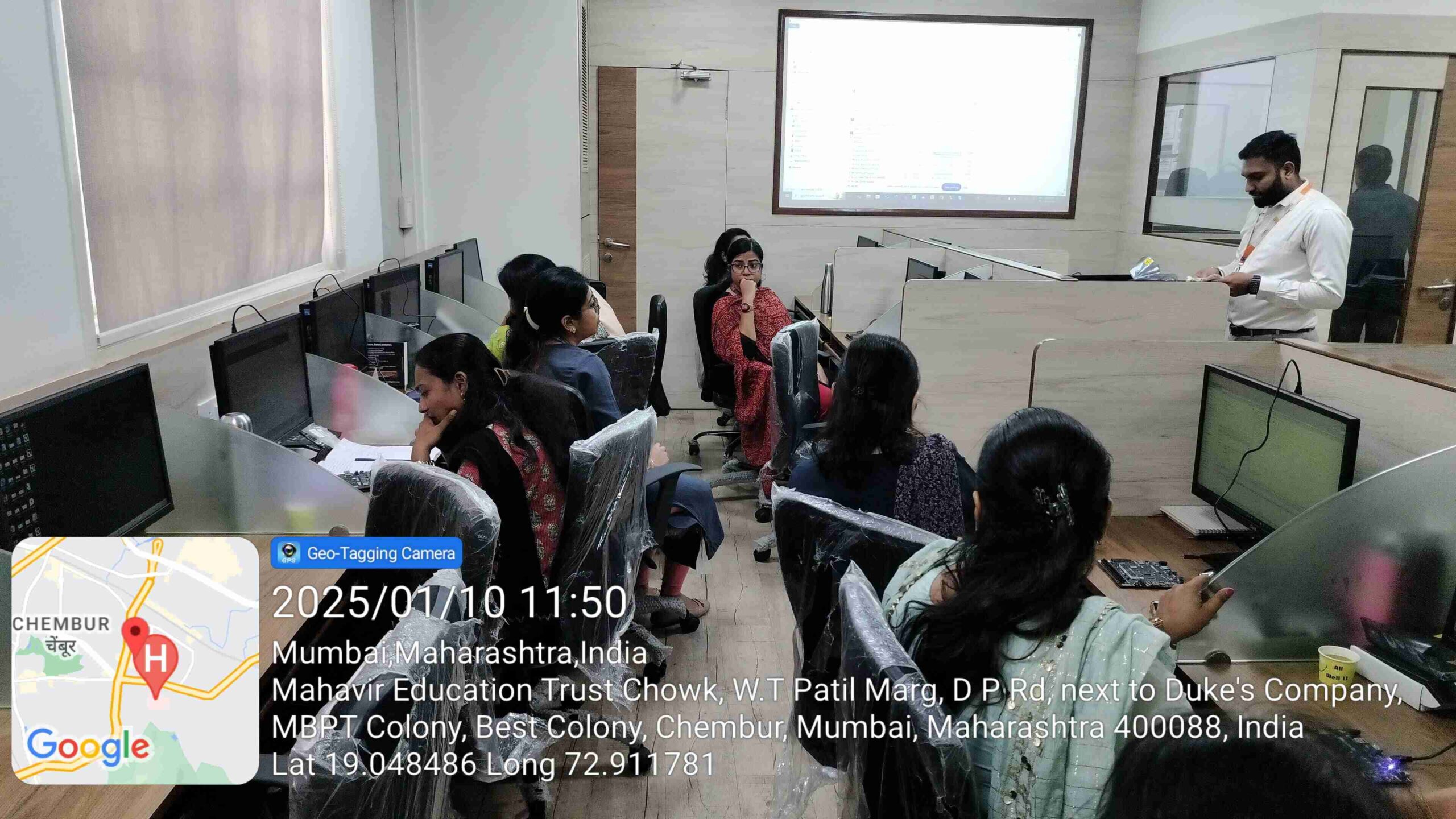
 Day 1–2: Software Training on LTM, Eagle software, PCB Express, easyEDA tool.
 Get trained directly by industry experts on latest PCB design tools and fabrication techniques
 Learning Outcomes:
 Understand the complete PCB design flow – schematic to prototype
 Why You Should Join:
 Best PCB Design
 Limited Seats Available — Register Early!

 Why Join Us?
 Hands-on Research & Projects
 Collaborations with NGOs, universities & industries
 Opportunities to present at conferences & publish research
 Mentorship from experienced faculty & domain experts
 Pre-interview Tasks:
 Important Dates
 Apply Now:
 Saachi Pandey – 7977364577
 📢 Ready to Shape the Future with AI?
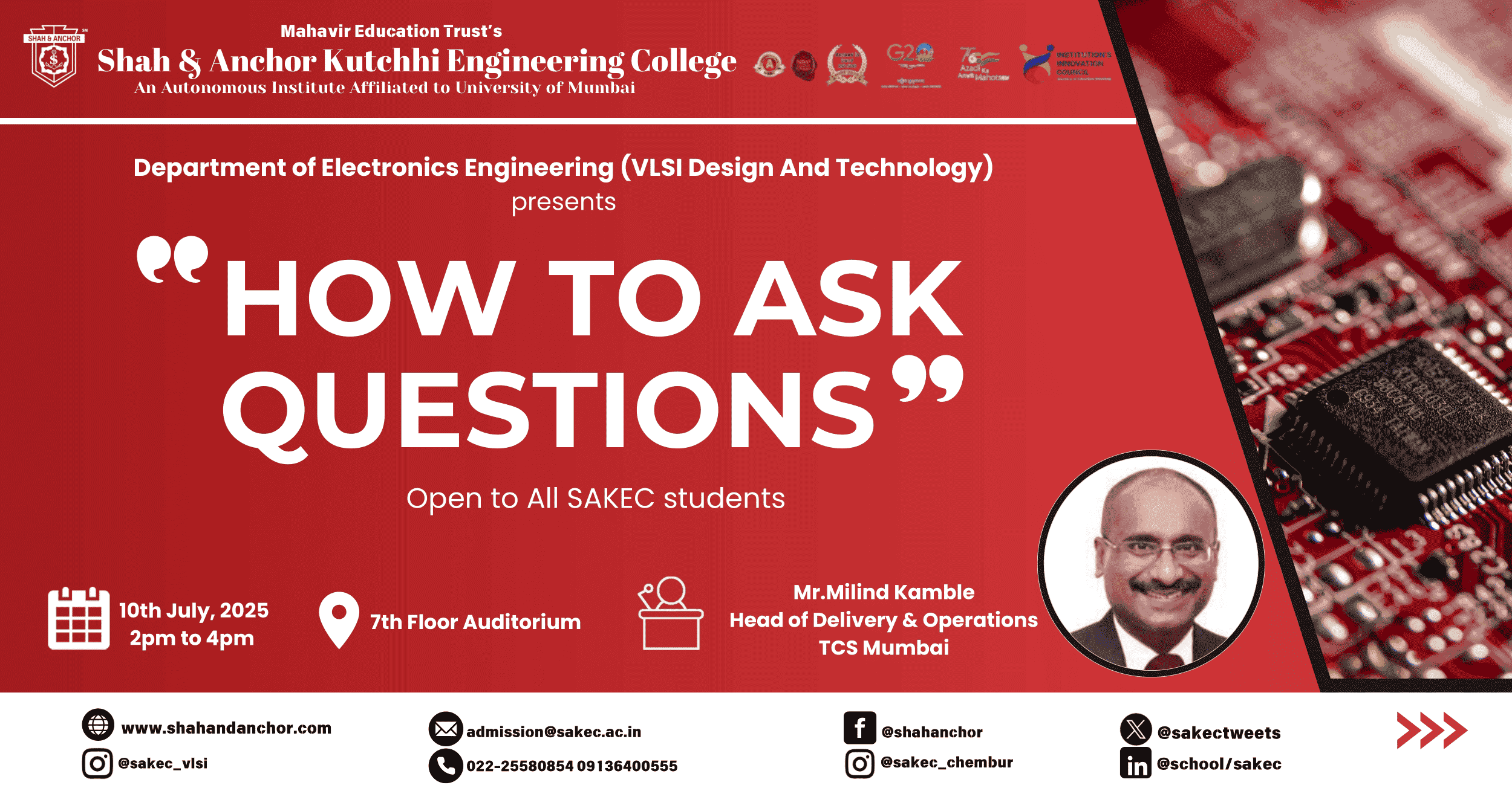

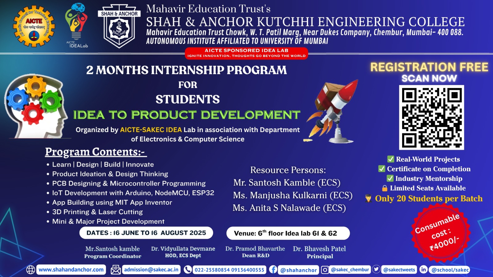 *Two months Summer Internship / Skill Development Program – 16/06/2025 to 16/08/2025*
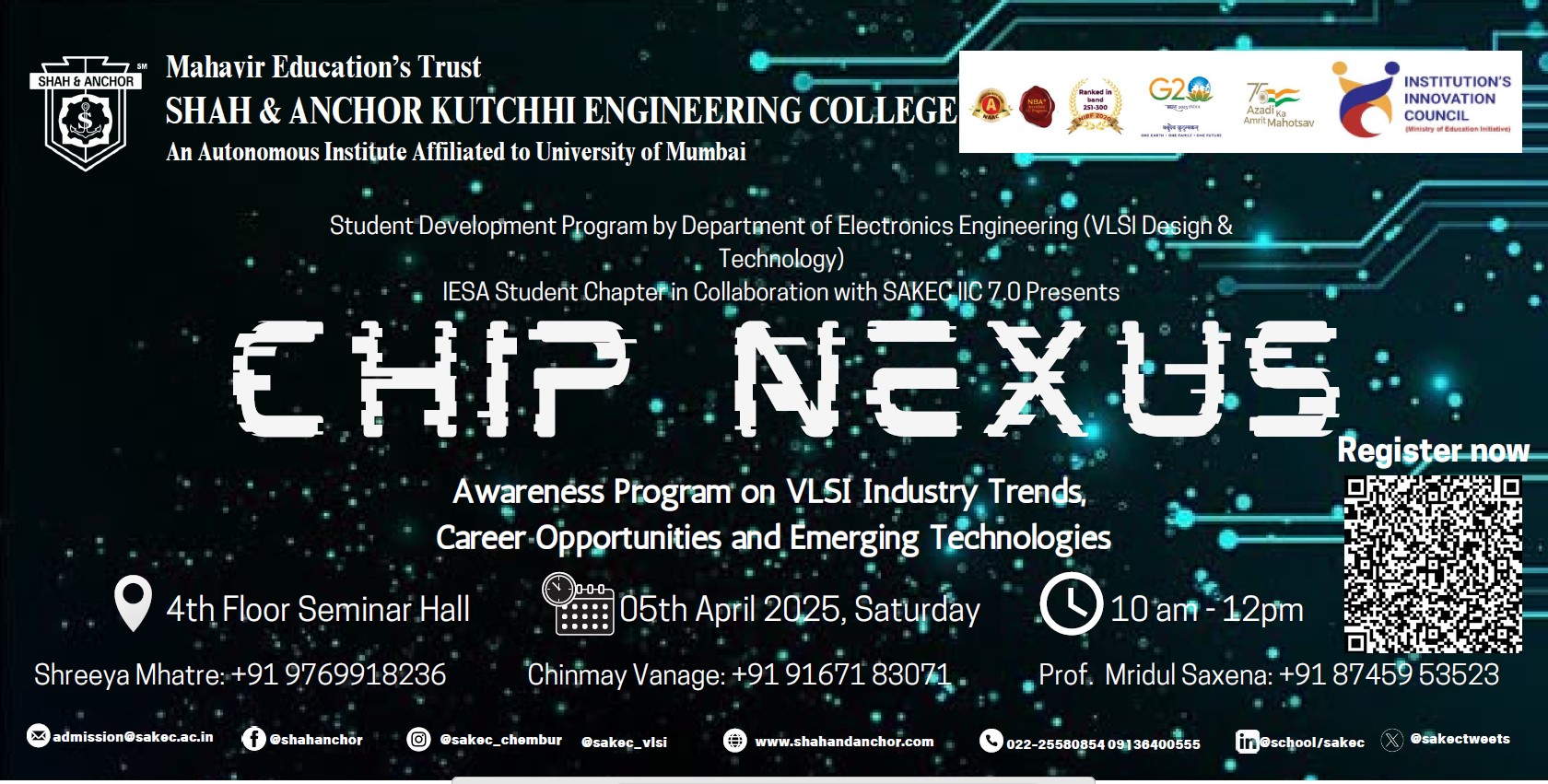
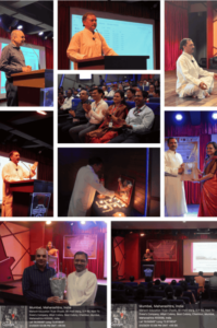
 Join Us for CHIP NEXUS – Your Gateway to the Future of VLSI!
 Department of Electronics Engineering (VLSI Design and Technology)
 Curious about the future of VLSI and semiconductor technology? Want to explore exciting career opportunities in this rapidly evolving industry? CHIP NEXUS is your chance to gain exclusive insights from industry experts!
 What to Expect?
 Explore career paths & job opportunities in the semiconductor industry
 Venue: 4th Floor Seminar Hall
 Time: 10 am to 12 pm
 Register Now & Secure Your Spot!: